
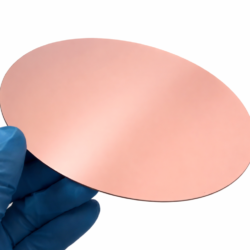
Copper-Coated Silicon Substrates (Cu/Ti on Si (100))
Price range: $29.00 through $89.00
Free shipping on orders over $100
- Satisfaction Guaranteed
Copper-Coated Silicon substrates (Cu/Ti on Si (100))
Overview
Our copper-coated silicon substrates are precision-cut from research-grade Cu thin film wafers fabricated on Si (100) substrates using high-vacuum magnetron sputtering.
A 10 nm titanium (Ti) adhesion layer is deposited between the silicon substrate and the copper film to ensure strong interfacial bonding and stable electrical performance.
These Cu-coated chips are widely used in electrochemical research, CO2 reduction studies, electrode development, and microfabrication experiments.
Layer Structure
Cu (Copper layer)
Ti (10 nm adhesion layer)
Si (100) substrate
Available Sizes
5 × 5 mm
10 × 10 mm
15 × 15 mm
Copper Thickness Options
100 nm – Recommended for general electrochemical research
200 nm – Recommended for enhanced stability
500 nm – Thick conductive layer for high-current applications
Substrate Specifications
Orientation: Si (100)
Doping: N-type, 1–10 Ω·cm resistivity
Surface finish: Single-side polished (SSP)
Deposition Process
High-vacuum magnetron sputtering
Controlled thickness uniformity
Precision wafer dicing
Clean-room compatible handling
Applications
CO2 reduction reaction (CO2RR)
Electrochemical catalysis research
Electrode platform development
Electroplating seed layer studies
Microelectronic interconnect research
Quality & Packaging
Uniform film thickness control
Research-grade surface quality
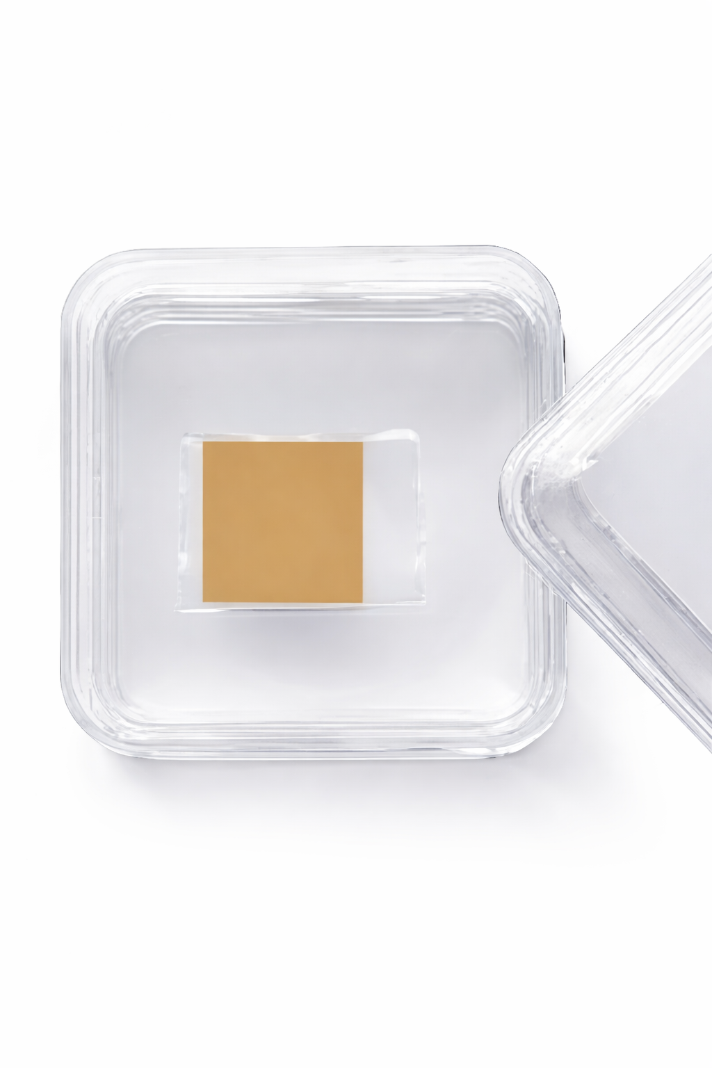
Protective packaging to minimize oxidation exposure
Custom sizes and thicknesses available upon request.
| option | 10 × 10 mm Si | 100 nm Cu, 10 × 10 mm Si | 200 nm Cu, 10 × 10 mm Si | 500 nm Cu, 15 × 15 mm Si | 100 nm Cu, 15 × 15 mm Si | 200 nm Cu, 5 × 5 mm Si | 100 nm Cu, 5 × 5 mm Si | 200 nm Cu |
|---|
Related products
-
Copper-Coated Silicon Wafers (Cu/Ti on Si (100))
Price range: $119.00 through $399.00