
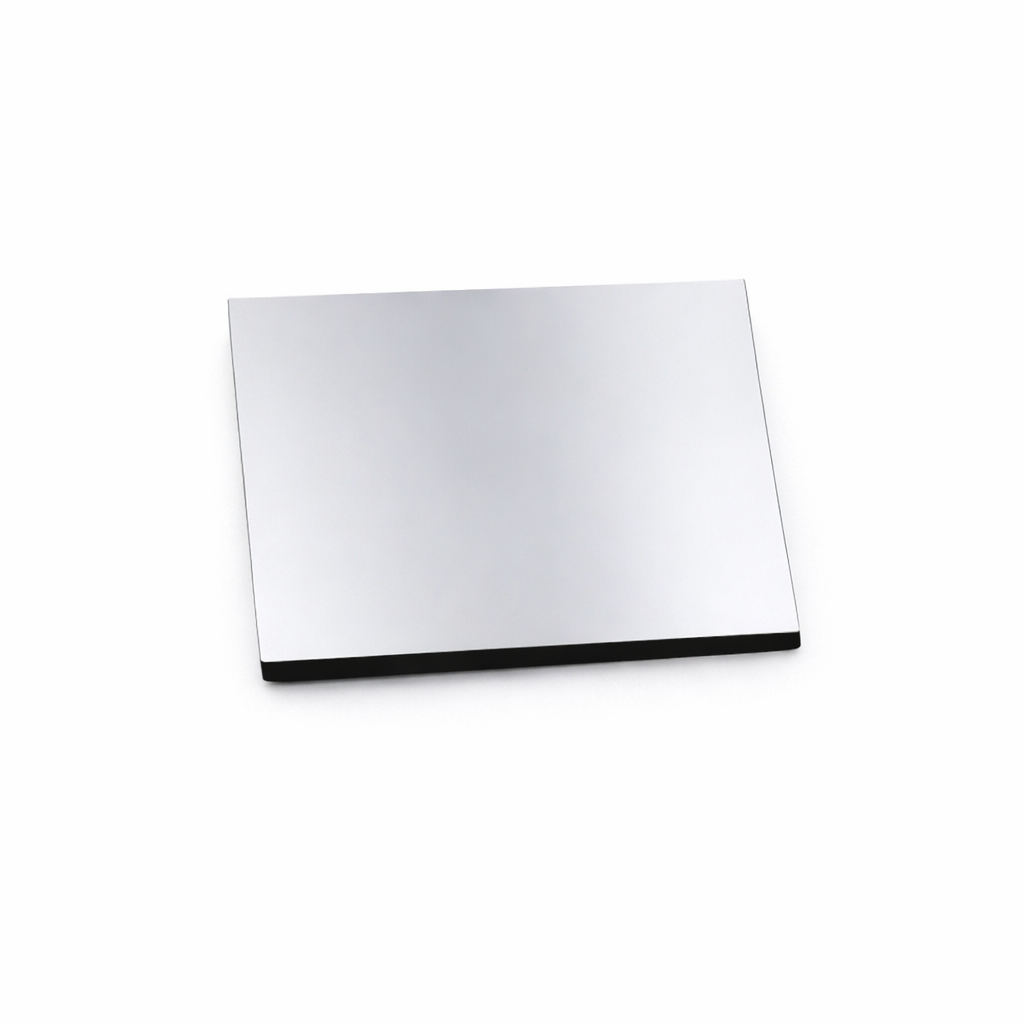
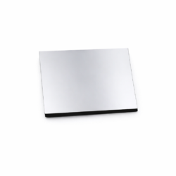
Silicon (Si) Single Crystal Substrates (N-type, doped), 10 pcs/pack
Price range: $79.00 through $129.00
Free shipping on orders over $100
- Satisfaction Guaranteed
Silicon (Si) Single Crystal Substrates (Wafers)
Physical Properties:
– Crystal Structure: Cubic System
– Lattice Constant: a=5.4301 Angstrom
– Hardness: 6.5 (Mohs)
– Density: 2.329 g/cm^3
– Melting Point: 1414 °C
– Growth Method: CZ and FZ
Standard Specifications:
1. Orientation Note
– Other orientations customizable
2. Surface Quality
– Polish: Single-side polished / Double-side polished
Silicon Wafer Grade Selection Guide
We offer two primary wafer grades for research and semiconductor applications: Research Grade and Prime Grade (Device Grade). Each grade is optimized for different experimental and fabrication needs.
Research Grade Silicon Wafers
(Also known as: Lab Grade / General Research Grade)
Description:
Research-grade silicon wafers are high-quality polished wafers designed for academic research, material science, thin film deposition, and general laboratory use. They provide excellent surface quality and flatness suitable for most non-device fabrication experiments.
Key Characteristics:
* High-quality single crystal silicon
* Single-side or double-side polished
* Good surface flatness and cleanliness
* Cost-effective for routine research
* Minor surface defects or particles may be present (non-device-critical)
* Not certified for integrated circuit fabrication
Recommended Applications
* Thin film deposition (Au, Pt, Ti, Al, etc.)
* 2D materials growth and transfer
* Optical and photonic experiments
* Surface chemistry and catalysis
* SEM/AFM characterization
* Electrochemistry substrates
* General university research
Best For:
Most academic and R&D laboratory use
—
Prime Grade Silicon Wafers (Device Grade)
(Semiconductor / IC / Device Fabrication Grade)
Description:
Prime-grade silicon wafers represent semiconductor industry device-grade quality. These wafers feature ultra-low surface roughness, extremely low defect density, and tightly controlled electrical and crystallographic specifications. Suitable for microfabrication, MEMS, and semiconductor device production.
Key Characteristics:
* Semiconductor device fabrication grade
* Ultra-low particle and defect density
* Excellent surface roughness (typically <0.5 nm Ra)
* Tight resistivity and orientation tolerance
* High uniformity across wafer
* Cleanroom-compatible packaging
* Suitable for photolithography and microfabrication
Recommended Applications:
* Micro/nano device fabrication
* MEMS processing
* Photolithography
* Semiconductor device research
* Epitaxy and thin-film growth requiring ultra-clean surfaces
* MOS/MIS structure fabrication
* Advanced university cleanroom use
Best For:
Device fabrication and high-precision semiconductor research
—
How to Choose the Right Grade:
Application Type | Recommended Grade
Thin film deposition | Research Grade
Catalysis / materials research | Research Grade
2D materials / graphene transfer | Research Grade
Optical experiments | Research Grade
SEM/AFM substrates | Research Grade
Teaching labs | Research Grade
Photolithography | Prime Grade
MEMS fabrication | Prime Grade
Semiconductor devices | Prime Grade
Epitaxy growth | Prime Grade
Cleanroom fabrication | Prime Grade
—
Quick Recommendation:
For 90% of university and lab research: Research Grade is sufficient
For device fabrication or cleanroom processing: Choose Prime Grade
| option | 10 × 10 × 0.5 mm,Double-side Polished,Research Grade, 10 × 10 × 0.5 mm,Single-side Polished,Research Grade, 20 × 20 × 0.5 mm,Double-side Polished,Research Grade, 20 × 20 × 0.5 mm,Single-side Polished,Research Grade, 5 × 5 × 0.5 mm,Double-side Polished,Research Grade, 5 × 5 × 0.5 mm,Single-side Polished,Research Grade |
|---|---|
| option2 | N-type (As-doped), N-type (Ph-doped), N-type (Sb-doped) |
Related products
-

Silicon (Si) Single Crystal Wafers (P-type, doped)
Price range: $29.00 through $9,999.00 -

Silicon (Si) Single Crystal Wafers (Undoped)
Price range: $29.00 through $9,999.00 -

Silicon (Si) Single Crystal Substrates (Undoped), 10 pcs/pack
Price range: $79.00 through $129.00 -
Silicon (Si) Single Crystal Substrates (P-type, doped), 5 pcs/pack
Price range: $79.00 through $129.00 -
Silicon (Si) Single Crystal Wafers (N-type, doped)
Price range: $29.00 through $9,999.00