
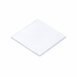
Gallium Nitride (GaN) Single Crystal Wafers, <0001>
Price range: $979.00 through $999.00
Free shipping on orders over $100
- Satisfaction Guaranteed
Gallium Nitride (GaN) Single Crystal Substrate
Physical Properties:
– Crystal Structure: Hexagonal System
– Lattice Constant: a=3.186Angstrom, c=5.186Angstrom
– Preparation Method: HVPE
Standard Specifications:
– Orientation: C-plane (0001) off angle toward M-axis 0.35° ± 0.15°
– Primary Flat: (10-10) ± 2.0° / 16 ± 1 mm
– Secondary Flat: (11-20) ± 3.0° / 8 ± 1 mm
– Dimensions: 5 x 5 x 0.4 mm, 10 x 10 x 0.4mm, dia50.8 x 0.4 mm
– Surface Finish: Single-Side Polished / Double-Side Polished
– Surface Roughness: Ra: < 0.5 nm – Effective Area: > 90%
Electrical Specifications by Type:
1. N-type/undoped:
– Resistivity: < 0.1 ohm-cm
2. N-type/Si-doped:
– Resistivity: < 0.05 ohm-cm 3. Semi-Insulating/Fe-doped: – Resistivity: > 1 x 10^6 ohm-cm
4. Semi-Insulating/C-doped:
– Resistivity: > 1 x 10^8 ohm-cm
| option | 2″ dia × 0.4 mm,N-type (Si-doped),Double-Side Polished, 2″ dia × 0.4 mm,N-type (Si-doped),Single-Side Polished, 2″ dia × 0.4 mm,N-type (undoped),Double-Side Polished, 2″ dia × 0.4 mm,N-type (undoped),Single-Side Polished, 2″ dia × 0.4 mm,Semi-Insulating (C-doped),Double-Side Polished, 2″ dia × 0.4 mm,Semi-Insulating (C-doped),Single-Side Polished, 2″ dia × 0.4 mm,Semi-Insulating (Fe-doped),Double-Side Polished, 2″ dia × 0.4 mm,Semi-Insulating (Fe-doped),Single-Side Polished |
|---|
Related products
-
GaN film on Sapphire Wafers
Price range: $495.00 through $505.00 -

GaN film on Sapphire Substrates
Price range: $62.00 through $131.00 -
Gallium Nitride (GaN) Single Crystal Substrates, <0001>
Price range: $459.00 through $699.00